
Adiuvo Engineering have recently designed a large, complex, space imaging FPGA, developing the majority of the code base in only a month. You might think that to do this we have cut corners and compromised quality, however, we haven’t. The question is how have we cut our development times down by a factor of 5, whilst maintaining the highest levels of quality?
To answer this in a single sentence: we have deployed a unique Model-Based Engineering (MBE) workflow for FPGA. An MBE workflow is one that uses models to define the technical baseline for a product. By using models, an engineer is able to work at a higher level, abstracting away much of the detailed work that is often time consuming and labor intensive. This type of approach not only helps to drive efficiency but also helps to improve quality. By raising the level of abstraction the engineer can handle large complex designs more effectively, focusing their effort on solving key technical challenges without becoming lost in the details.
The design in question is a large video processing design that has been developed for a major multi-national company. The design uses a Microchip PolarFire FPGA, filling one of the larger devices. The design is intended for use in space and therefore must be developed to the highest standards of quality and reliability. The design drives a high-end scientific CMOS image sensor, processing the resulting video, before driving it out over a high-speed serial interface. The design includes over 100,000 single lines of VHDL code, most of which were generated in only a month by utilizing model-based techniques.

So what does our FPGA development process look like? Well it might surprise you to hear, but we only see designing the FPGA as a small part of our overall process. When developing FPGAs at Adiuvo we use a rigorous requirements-driven FPGA development flow that is inspired by standards such as DO-254. The most important aspect of such a workflow is that everything is driven from a formal set of robust requirements. We typically spend quite a sizable portion of a project on ‘front-end’ systems engineering tasks that we use to support the development of robust FPGA level requirements. We believe that it is important to not only generate formal requirements, but to ensure that they are supported by rigorous system-level analysis to ensure that the requirements are also robust.

As well as the front-end activities, we also put a lot of emphasis on the ‘back-end’ verification and validation activities, typically spending over half of our time on these critical, but often overlooked activities. These activities can help us to ensure that our designs meet the requirements that we have defined (verification), and also that we have the correct requirements in the first place (validation).
So how do we use model-based engineering in such a process? Well in outline we use two main types of models at Adiuvo Engineering: SysML models for higher-level modelling and Simulink models for lower-level modelling. We tend to use SysML in the earlier phases of our lifecycle before transitioning over to Simulink in the later phases of the lifecycle.
SysML is a general purpose modelling language that was developed to support systems engineering activities. However, the semantics of SysML are well suited to describing hardware, and FPGAs in particular. SysML models are static models that are used to describe the structure and behavior of a system. They are not numerical models that can be executed and simulated. At Adiuvo we used SysML models in three main ways: to help us perform systems engineering, to help us analyze and write requirements, and to help us generate the FPGA concept design.

One of the key things that we have developed is a custom workflow that allows us to code generate our FPGA structures from a SysML model. Our workflow typically starts with us developing a ‘system level’ model that allows us to explore issues at the system level and to help us understand the context in which the FPGA is operating. This system level model is then evolved into a requirements model for the FPGA that captures the primary FPGA requirements. The FPGA requirements model is itself then converted into a detailed FPGA architectural design, also captured in SysML. To help drive maximum benefit from such a workflow, we have developed a set of custom code generation tools that allow us to turn our FPGA architectural model into VHDL that describes our high-level device structure. This process will automatically insert things like AXI networks and will also create all of the structural (VHDL) code for our FPGA. By doing this we can not only save time, but also ensure that we have a robust design that traces directly back to our requirements and also to the higher level system design.

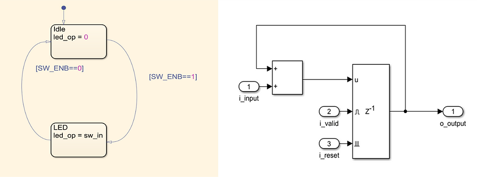
Once we have the FPGA architectural design in place, we then switch to using Simulink. We use Simulink in two main ways: to generate the functional (block level) code for our design and to generate our low-level test benches and test-cases. Our workflow in Simulink typically involves prototyping algorithms or higher-level concepts in Matlab, before then moving into Simulink to develop our FPGA block designs. Simulink is well suited to FPGA design as you can model not only digital signal processing, but also model things like finite state machines and combinatorial logic. Once we have our Simulink model for a block we then develop a test-bench and test-cases for the block in Simulink. We often use our initial Matlab concept as a ‘golden model’ that we can use to verify the correctness of our detailed Simulink implementation. Once we have generated our block and verified its operation, we then use Simulink HDL Coder to generate VHDL code. This VHDL code is then integrated into our high-level device framework that we generated using SysML.
We also employ continuous integration throughout this approach. We use tools such as Jenkins to allow us to automatically run processes such as verification, device implementation, and linting on a regular basis (typically nightly). By doing this we can ensure that our code base is always robust, checking that our design still synthesizes and closes timing, whilst also checking that our test-cases pass. By running automated linting checks on our code based we also ensure that our code is of highest quality and that issues such as clock-domain crossing problems are caught early.
Overall, by deploying a process that focusses on the front-end of the lifecycle, and which uses techniques such as model-based design and continuous integration, we are able to significantly reduce our overall development timeframes. We also believe that this approach produces the high quality designs suitable for the most challenging of applications.
I'm wondering whether you manage requirements directly in the SysML tool or with a dedicated requirement tool and also how do you manage traceability of requirements vs simulink model, considering the two tools do not speak to each other.
Thank you