MicroZed Chronicles: AXI Virtual FIFO Controller
- Adam Taylor

- Mar 30, 2022
- 3 min read
FIFOs are versatile tools to use within our designs because they enable us to buffer data when doing signal and image processing. We also use the asynchronous version to perform clock domain crossing for data buses.

One of the challenges with FIFO is that storing large amounts of data requires significant resources within the FPGA. This can be an issue in smaller FPGAs, of course, because BRAM resources are limited. In many instances though, smaller FPGAs may have external memories connected like DDR3 or DDR3L. Developers can use this memory to buffer signals externally in the DDR memory using Direct Memory Access (DMA). This does require overhead to set up the DMA accesses and complicates the solution.
AMD-Xilinx provides an IP core called the AXI Virtual FIFO Controller to simplify the situation when developers want to use the DDR memory to store signal or data samples in external DDR as a FIFO.
The AXI Virtual FIFO Controller provides the developer with master and slave AXI stream ports that can be connected to the signal processing path. The interface with the DDR memory is then provided by a full AXI interface.

Using these interfaces, the Virtual FIFO Controller is able to create a FIFO within the DDR and is capable of storing larger quantities of data than can be implemented using internal BRAM.
The Virtual FIFO Controller provides the ability to have several channels stored in the external DDR. The configuration of the IP block enables the address range to be used in the DDR for the data. One thing to be careful with is clashing memory locations with other memory uses (e.g., MicroBlaze applications). Within the IP customization, we are able to define the allocated space for the samples within the IP customization. These are defined in 4 KB blocks.

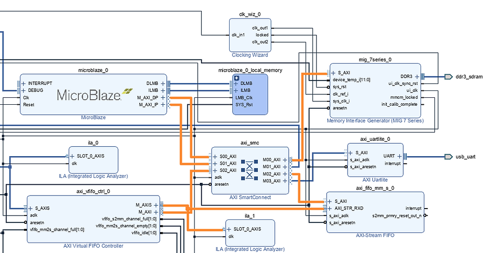
I created a small project that targets the Arty S7-50 to demonstrate how the AXI Virtual FIFO Controller works. In this design, the XADC is the source of the AXI Stream data to be written into the DDR which can output its samples over AXI Stream.
The output (read channel) from the AXI Virtual FIFO Controller is connected to a AXI Stream FIFO and configured for data to be read over AXI4-Lite interface.
The input path in the design is shown below with signals generated by the XADC and a subset convertor used to add in TLast signal to the AXI Stream. The AXI ILA enables the data generated from the XADC to be checked against what we see in the DDR memory later. The signal then passes through the AXI Virtual FIFO Controller to a Smart Interconnect Controller and into the MIG.

The output path is similar. It goes from the MIG through the SMC and into the AXI Virtual FIFO Controller and out to the AXI Stream FIFO where it can be accessed by the MicroBlaze.

When this was downloaded onto the Arty S7-50, we can run a simple hello world application, pause the program, and observe the DDR memory location where the AXI Virtual FIFO Controller is buffering data.

This data can be confirmed by observing the first ILA in the Vivado hardware manager. We could have configured cross probing for extra verification.

The output path requires the AXI Stream FIFO asserting the Tready signal. To do this, we need to configure the AXI Stream FIFO using software running on the MicroBlaze. We will examine the AXI Stream FIFO configuration in the next blog because it’s also an interesting IP core with capabilities we should be aware of.


Comments