
MicroZed Chronicles: Leonidas Board
- Adam Taylor
- Nov 29, 2023
- 4 min read
Learning how to develop FPGAs and embedded systems can be a challenge so I like to think that this blog has provided significant support and knowledge to those who need it over the years. One of the things I’ve wanted to do is create our own development board which helps engineers learn.
A few weeks ago, we looked at how we could create our own board definition based around an open-source development board. This is the board we’ve been developing and we’ll be making the schematics open source once we’ve tested revision B of the design.

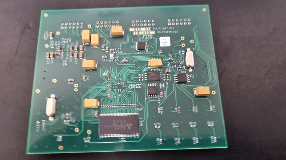
The board which I call Leonidas as king of the Spartans, has been designed to support a range of developments from simple logic and embedded system development, to more complex solutions such as image processing basics.
The board itself includes a Spartan 7 FPGA with a FTGB196 pin package which provides 100 user IO. This footprint provides a XC7S6 to the XC7S50, providing between 6000 logic cells to 52160 logic cells.
Connected to the FPGA is a FTDI232H which enables Vivado to program the FTDI chip so that we can configure either the FPGA device directly or its configuration PROM. The boot method is determined by a jumper which selects either JTAG or PROM.
Along with the configuration PROM, the FPGA is connected to a SDRAM which provides 64 Mbit of memory. We selected SDRAM because a DDR controller would take up most of the logic like in the smaller devices. SDRAM, however, can be implemented pretty easily and leaves a lot of logic to spare for other developments. It is also a good teaching exercise to develop a SDRAM controller. The FPGA also provides a SPI flash memory for developers to store application data in, which is separate to the configuration memory.
As would be expected with a development board, it also provides switches, push buttons and LEDs. Interface wise, three Pmods are connected to the FPGA IO and these are tracked for high-speed differential. One of the Pmods has an optional LVDS transceiver which provides two transmit and two receive channels. This is intended for non-Pmod type applications where a high-speed LVDS is required.
A 100 MHz reference clock is provided to ensure a wide range of clocking options.
What makes this board slightly different from others is the inclusion of a Raspberry Pi RP2040 which provides dual-core Arm M0+ cores running at 133 MHz. This provides a USB interface to the wider world and is also connected to the FPGA. This allows the FPGA to act as an IO expander or accelerator if the application requires it.
To get started with the board, I thought I would create a simple design which displays a count and outputs it over a UART. This UART data will be received by the RPI Pico and output to a terminal. Since I am curious how small I can get a MicroBlaze, I am going to use it to provide the functionality in the FPGA.
Luckily, I have already created a board definition and installed it within Vivado. This means we are able to create a project which is already board aware.


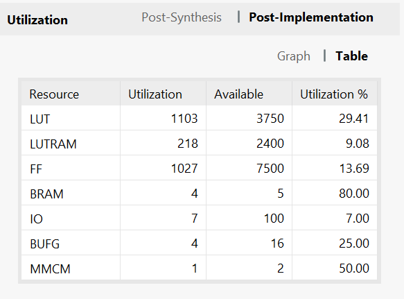
I have created an IP integrator block diagram into the newly created project and added in the MicroBlaze (click here for very detailed MicroBlaze Instructions). Unlike previous MicroBlaze instantiations, I have set the optimization to AREA to ensure it uses the smallest number of resources possible. I am going to use 16 KB of memory and only the AXI Data Peripheral Interface.
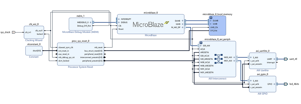
I used the board definition to connect the GPIO LEDs and added the UART manually but will make sure to update the production files to include a UART along with I2C and SPI connections to the PICO.
Once the hardware bit stream is generated, we are able to export the hardware and create a new project in Vitis (detailed guide here).


I used the unified IDE in Vitis to create a platform and application. The application software is very simple as it just drives the LEDS to toggle on a half-second cycle. It also outputs a count once every second over the UART.
#include <stdio.h>
#include "platform.h"
#include "xil_printf.h"
#include "xparameters.h"
#include "xgpio.h"

XGpio LEDS;

int main()
{
    init_platform();
    print("Vitis Unified IDE Example\n\r");
    XGpio_Initialize(&LEDS, XPAR_XGPIO_0_BASEADDR);
    int count;

    XGpio_SetDataDirection(&LEDS, 1, 0x0 );
    count = 0;

    while(1){
        XGpio_DiscreteWrite(&LEDS, 1, 0x00);
        xil_printf("%2x", count);
        usleep(500000);
        XGpio_DiscreteWrite(&LEDS, 1, 0x0f);
        count++;
        usleep(500000);
        XGpio_DiscreteWrite(&LEDS, 1, 0x00);

        usleep(500000);
    }


    cleanup_platform();
    return 0;
}
Once this is working, we can download and execute the source code on the MicroBlaze and we should see the lights flashing.
If we connect to the RP2040 and download the MicroPython below, we will also see the UART data being received.
import machine
import utime
import ustruct
import sys
from machine import UART, Pin
uart0 = UART(0, baudrate=9600, tx=Pin(0), rx=Pin(1))
while True:
    utime.sleep(1)
    data = uart0.read(2)         # read up to 5 bytes
    print("Pattern over UART From FPGA",data)
Of course, this is a fairly simple example but it does show the flexibility of the development board.

One of the things I am keen to get up and running is our SPI/I2C/UART to AXI IP which enables the RPI Pico to access peripherals within the FPGA and uses a AXI Interconnect as outlined in this project on Hackster!
You can find the schematics for the design here.
Workshops and Webinars
If you enjoyed the blog why not take a look at the free webinars, workshops and training courses we have created over the years. Highlights include
Professional PYNQ Learn how to use PYNQ in your developments
Introduction to Vivado learn how to use AMD Vivado
Ultra96, MiniZed & ZU1 three day course looking at HW, SW and Petalinux
Arty Z7-20 Class looking at HW, SW and Petalinux
Mastering MicroBlaze learn how to create MicroBlaze solutions
HLS Hero Workshop learn how to create High Level Synthesis based solutions
Perfecting Petalinux learn how to create and work with petalinux OS
Embedded System Book Do you want to know more about designing embedded systems from scratch? Check out our book on creating embedded systems. This book will walk you through all the stages of requirements, architecture, component selection, schematics, layout, and FPGA / software design. We designed and manufactured the board at the heart of the book! The schematics and layout are available in Altium here Learn more about the board (see previous blogs on Bring up, DDR validation, USB, Sensors) and view the schematics here.
Sponsored by AMD
Hi @Adam I just saw this board in-person last week for the first time and it would be perfect for my next DIY project I have underway.
How can I purchase some of these boards?