
MicroZed Chronicles: Turning Concepts into Reality, The FPGA Screen Challenge
- Adam Taylor
- Sep 4, 2024
- 4 min read
A few weeks ago, I outlined several beginner-friendly FPGA projects to help you get started with your chosen development language.
Today, we’re going to take things up a notch and dive into a more complex design project that mirrors real-world scenarios. This project isn’t just about honing your technical skills; it’s about mastering the entire FPGA development process, from concept to implementation.
I’ll be sharing my solution to this project as a Hackster post in the near future, likely in the new year, because doing this right takes time and patience. This project idea originally came from our previous Chief Engineer as a way to onboard new graduates, and it's proven to be an invaluable learning tool.
Project Objectives
The goal of this project is twofold: first, to equip engineers with the necessary technical FPGA skills, and second, to provide hands-on experience with the entire development lifecycle. Here’s what you’ll be learning:
Tools and Techniques: An introduction to the tools and techniques used in FPGA development.
Development Lifecycle: Exposure to the entire FPGA development lifecycle, from concept to hardware testing.
Process Understanding: A deep dive into the specific FPGA development processes used in professional environments.
Real-World Experience: Working on a project that closely resembles real-world FPGA tasks, beyond what you might encounter in a university course.
Project Overview
The task is to use an AMD development board to produce an SMPTE colour bars test pattern on a full-HD (1920x1080) monitor using an HDMI output from the board.

To ensure this project is sufficiently challenging, the design must be created from scratch—you won’t be using existing IP blocks provided by Vivado. While these IP blocks can accelerate development, the objective here is to teach newer engineers the skills necessary to create their own IP blocks. Mastering this process is invaluable, especially when working on projects that do involve IP blocks and require meticulous planning, estimation, and requirement gathering.
Project Requirements
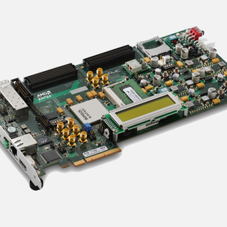
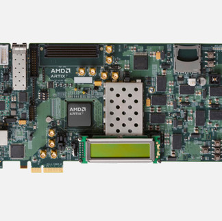
You can use any AMD development board with an HDMI output for this project, but to make things more interesting, choose a board with an HDMI ADV7511 Transmitter. This adds an extra layer of challenge by requiring you to set up the HDMI Transmitter over I2C. The Arty Z7 and Zybo Z7 can also be used along with the PYNQ Z1 and Z2


Tools Needed
You’ll need the following tools to complete the project:
Development Tools:
Source Control:
Design Tools:
Draw.io: For drawing diagrams and architectures.
Google Docs / MS Office / LibreOffice: For documentation and planning.
Project Management (Optional):
Jira, Confluence, Enterprise Architect: For planning, documentation, and generating requirements/architecture.
Project Stages
Here’s a step-by-step breakdown of how you should approach this project:
Set Up Source Control: Start by setting up a repository in your chosen source control tool.
Conceptual Design: Use Draw.io and your office suite to create a high-level concept of your design. This concept serves as the foundation for all subsequent stages.
Task Breakdown: Break down the project into individual tasks. If using Jira, represent each major process step as an Epic, with each task planned as a Story. Aim for each Story to take a few days of work.
Project Estimation: Estimate the time required for each task based on your concept design. Time estimates should be in hours, providing a realistic project timeline.
Project Planning: Create a time-phased project plan in Excel or a scheduling tool like Jira or MS Project.
Requirements Specification: Develop a detailed requirements specification that outlines the technical requirements for your design.
Detailed Architecture: Design the architecture for your project, showing all major blocks and their interfaces, including externally accessible registers. Tools like Draw.io and Enterprise Architect are particularly useful here.
Code Development: Write the RTL code for each block using VS Code.
Test Bench Creation: Develop a VHDL test bench and test cases to simulate your design in the Vivado Simulator.
Implementation: Implement your code in a Vivado project to generate a build for your development board.
Hardware Testing: Test your design on hardware, using Integrated Logic Analysers if needed for debugging.
Tools Breakdown by Stage

Conclusion
This project offers a comprehensive walkthrough of both the technical and process-oriented aspects of FPGA development. While writing code is crucial, mastering the full development process—including estimation, documentation, and planning—is equally important. For fresh graduates, I typically allocate several weeks to a few months for this project to ensure it’s completed successfully.
If your company doesn’t have a design process for VHDL/Verilog development, consider adopting one from Adiuvo. If you decide to take on this challenge, I’m happy to provide pointers and reviews along the way. Good luck, and remember—don’t be tempted to cut corners! The "boring" elements are just as crucial as the technical skills.
Workshops and Webinars
If you enjoyed the blog why not take a look at the free webinars, workshops and training courses we have created over the years. Highlights include
Professional PYNQ Learn how to use PYNQ in your developments
Introduction to Vivado learn how to use AMD Vivado
Ultra96, MiniZed & ZU1 three day course looking at HW, SW and PetaLinux
Arty Z7-20 Class looking at HW, SW and PetaLinux
Mastering MicroBlaze learn how to create MicroBlaze solutions
HLS Hero Workshop learn how to create High Level Synthesis based solutions
Perfecting Petalinux learn how to create and work with PetaLinux OS
Boards
Get an Adiuvo development board
Adiuvo Spartan 7 / RPi 2040 Embedded System Development Board
Embedded System Book
Do you want to know more about designing embedded systems from scratch? Check out our book on creating embedded systems. This book will walk you through all the stages of requirements, architecture, component selection, schematics, layout, and FPGA / software design. We designed and manufactured the board at the heart of the book! The schematics and layout are available in Altium here Learn more about the board (see previous blogs on Bring up, DDR validation, USB, Sensors) and view the schematics here.