MicroZed Chronicles: Versal Part Two – Device Architecture
- Adam Taylor
- Jan 19, 2022
- 3 min read
In the first instalment of this Versal miniseries, I briefly introduced the architecture of the Versal devices before showing a simple application build and Hello World. This provided a good introduction to the development flow. In this blog, I want to delve into the architecture and functional blocks contained within the Versal device and their primary capabilities. This will allow us to do deep dives into specific elements in future blogs.

Let’s look at the specific elements of the architecture.
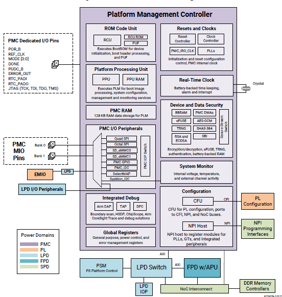
Platform Management Controller (PMC) – This manages the overall platform. It provides configuration, bring up, platform management during operation, and enables and facilities the system wide debug and tracing. To do this, the PMC has two processors. The ROM Control Unit (RCU) executes the initial stages of the boot and runs the boot ROM, while the PMC Processing Unit (PPU) loads in the Programmable Device Image (PDI) and the PDI replaces the BIN file used to configure earlier SoCs. The PDI contains several different files including the Platform Loader and Manager (PLM) which loads and processes the different files to configure the device. This includes the CDO files which configure the PMC, PS, Clocking, MIO and Reset. The NPI file configures the NOC, AI Engines, PL, and DDR Controller. Finally, the ELF files are loaded for the processors to begin the application.

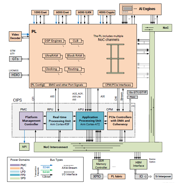
Application Processor Unit (APU) – This contains dual core 64-bit Arm A72 processors which support superscalar, out-of-order execution and implement the Arm-v8A architecture. Each of the processors has 48 KB of L1 instruction cache and 32 KB of data cache, and both have protection from errors parity on the instruction and ECC on the data. The processors also provide floating-point units and NEON units to provide Single Instruction Multiple Data processing. The L2 cache is 1 MB and connected to the cache coherent interconnect and controlled by the Snoop Control Unit.

Real-Time Application Unit (RPU) – Intended to enable the implementation of functional safety applications, the RPU provides dual 32-bit Cortex-R5F processors based on Arm-v7r architecture and include a floating-point unit. Each processor has 32 KB of L1 cache and tightly coupled memories with single-cycle read access. The TCM can be configured in two structures. In performance mode, the processors are independent and each processor has 128 KB of TCM. In lockstep mode, the processor is running in safety mode and 256 KB of TCM is provided.

I/O Peripheral (IOP) – The I/O peripherals are routed through the PS low-power domain or PMC Multiplexed IO (MIO). These MIO signals provide access from the PS to a range of standard peripherals including SPI, I2C, GPIO, CAN FD, UART, GigE, USB 2.0, QSPI, OSPI and eMMC. These interfaces enable us to work and interface with standard industry interfaces. The I/O peripherals, however, do not define the limits of the high-performance interfacing in Versal.
Network on Chip (NOC) – The NOC spans the entire device and is AXI4-based network capable of routing high bandwidth, real-time, and low-latency connections. The major NOC connections are the DDR controllers, PS to PL, PL to PL, and AI engine access.

Programmable Logic – This contains the high-performance parallel structures to implement custom high-speed designs. It mainly consists of DPS engines, configurable logic blocks and block memory, and UltraRAM. Connections between the PL and the PS domain are via either AXI interfaces (e.g., AXI4-Lite, AXI, ACE, ACP or the Network on Chip). Within the PL itself, there are several NOC channels which can be connected to. The PL also has interfaces to the AI engines and provides the integrated peripherals.
Integrated Peripherals – The integrated peripherals are the device options which are included in the PL fabric. These peripherals include the 100 G Ethernet MAC, 600 G Channelized Ethernet, 600 G Interlaken, 400 G Crypto Engine, Video Decoder Unit, and GTM transceivers.
Integrated Hardware Options – In addition to the integrated peripherals, Versal devices have integrated hardware options across the range of devices. These include the AI engines, accelerator RAM, coherency for PCIe module with CCIX, coherency for PCIe module with CXL, and high-bandwidth memory interface. Both the coherency for PCIe module with CCIX and coherency for PCIe module with CXL are referred to as the CPM in the block diagram (coherent module with PCIe).
Now we understand a little more about each of the key blocks of the device. In the next blogs, we will look at elements such as the global address spaces, power domains, and inter-processor communication channels.

Commentaires